How Do Solar Panels Work? From Sunlight to Usable Electricity Step by Step
Step-by-step explanation of how solar panels work: photon absorption in silicon, the photovoltaic effect at the P-N junction, DC current, and inverter conversion.
By M. Khalif | Published 2026-11-18 | Updated 2026-11-18
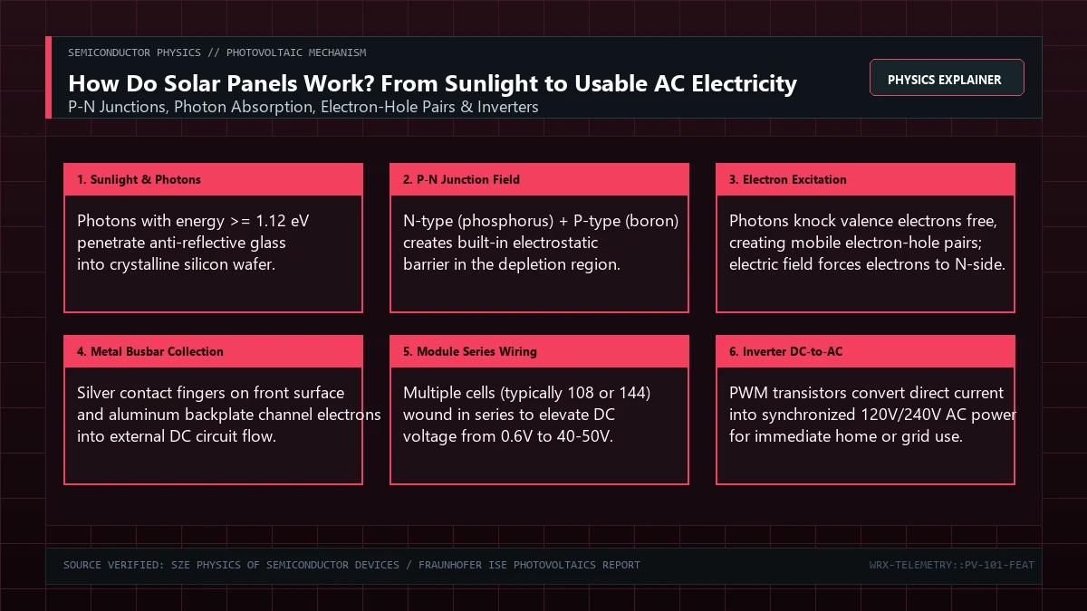
At first glance, a solar panel appears deceptively simple: a silent, motionless pane of dark glass framed in aluminum, producing clean electricity whenever sunlight touches it. There are no spinning turbines, no chemical combustion reactions, and no gears. Yet inside that wafer of silicon lies an extraordinary triumph of solid-state quantum physics that converts electromagnetic radiation directly into electrical energy: the photovoltaic effect.
Discovered by French physicist Edmond Becquerel in 1839 and theoretically explained by Albert Einstein in 1905 (for which he won the Nobel Prize in Physics), the photovoltaic effect operates at the subatomic scale. Packets of solar energy called photons collide with semiconductor atoms, knocking electrons free from their crystalline chemical bonds. A microscopic internal electric field built into the silicon forces those liberated electrons to flow in a single direction, generating a continuous direct electrical current (DC) that an inverter transforms into the alternating current (AC) electricity that powers your lights, appliances, and home. This guide explains the step-by-step physics and engineering of how solar panels work.
Step 1: Semiconductor Chemistry and Atomic Silicon Doping
To understand how a solar panel works, one must start with the atomic structure of silicon (Si). Silicon is a semiconductor material with four valence electrons in its outer shell. In pure crystalline silicon, every silicon atom forms covalent bonds with four neighboring silicon atoms, creating a stable diamond cubic lattice. Because all valence electrons are tightly locked in covalent bonds, pure silicon is a poor electrical conductor at room temperature.
To make silicon conduct electricity when exposed to light, engineers deliberately introduce minute trace impurities—a chemical process called doping:
1. N-Type Silicon (Negative Layer): The top surface of the wafer is doped with an element that has five valence electrons, typically phosphorus (P). Four of phosphorus's electrons bond with adjacent silicon atoms, leaving the fifth electron loosely bound and free to move throughout the conduction band. Because it has surplus mobile negative charge carriers, this is designated the N-type layer.
2. P-Type Silicon (Positive Layer): The base layer of the wafer is doped with an element having three valence electrons, typically boron (B) or gallium (Ga). Boron has one less electron than silicon, creating an electron vacancy or 'hole' in the crystal lattice. These holes act as mobile positive charge carriers that can accept free electrons, designating this the P-type layer.
Step 2: The P-N Junction and the Internal Electric Field
When N-type and P-type silicon are joined together, a dynamic physical boundary called the P-N junction forms between them. Free electrons from the N-side immediately diffuse across the boundary to fill adjacent holes on the P-side.
As electrons cross the junction, they leave behind positively charged ionized phosphorus donor atoms in the N-layer. Conversely, the incoming electrons create negatively charged ionized boron acceptor atoms in the P-layer. This migration quickly creates a microscopic barrier called the Depletion Region (so named because it is depleted of mobile charge carriers).
The fixed positive ions on the N-side and fixed negative ions on the P-side establish a permanent, built-in electrostatic barrier (an internal electric field) across the junction, typically measuring 0.6 to 0.7 Volts. This electric field acts like a one-way electrical turnstile: it permits electrons to move only from the P-side toward the N-side, while pushing positive holes toward the P-side.
Step 3: Photon Absorption and the Photovoltaic Effect
Sunlight consists of a continuous stream of energy packets called photons. When sunlight strikes the solar panel, photons penetrate the anti-reflective glass into the silicon wafer. What happens next depends on the photon's energy level relative to silicon's bandgap energy:
• The Silicon Bandgap (E_g): At room temperature, crystalline silicon has an energy bandgap of approximately 1.12 electron-volts (eV)—the energy required to promote an electron from the bound valence band across the forbidden gap into the conductive conduction band. • Sub-Bandgap Photons: Photons with energy less than 1.12 eV (long-wavelength infrared light) lack sufficient energy to excite electrons; they pass through the silicon or dissipate as low-grade heat. • Absorption and Pair Generation: When a photon with energy equal to or greater than 1.12 eV strikes a bound valence electron, the electron absorbs the photon's energy and jumps into the conduction band. This excitation leaves behind an empty hole, creating an electron-hole pair (an exciton). • Charge Separation: Under normal circumstances, an excited electron would quickly lose its energy and recombine with a hole. However, if the electron-hole pair is created near the P-N junction, the permanent internal electric field immediately pulls the electron to the N-side and pushes the hole to the P-side before they can recombine. This physical separation of charges creates an electrical voltage potential across the cell.
Step 4: Metal Contacts, Busbars and Cell-to-Module Wiring
To extract these separated electrons and perform useful electrical work, the cell must be connected to an external circuit:
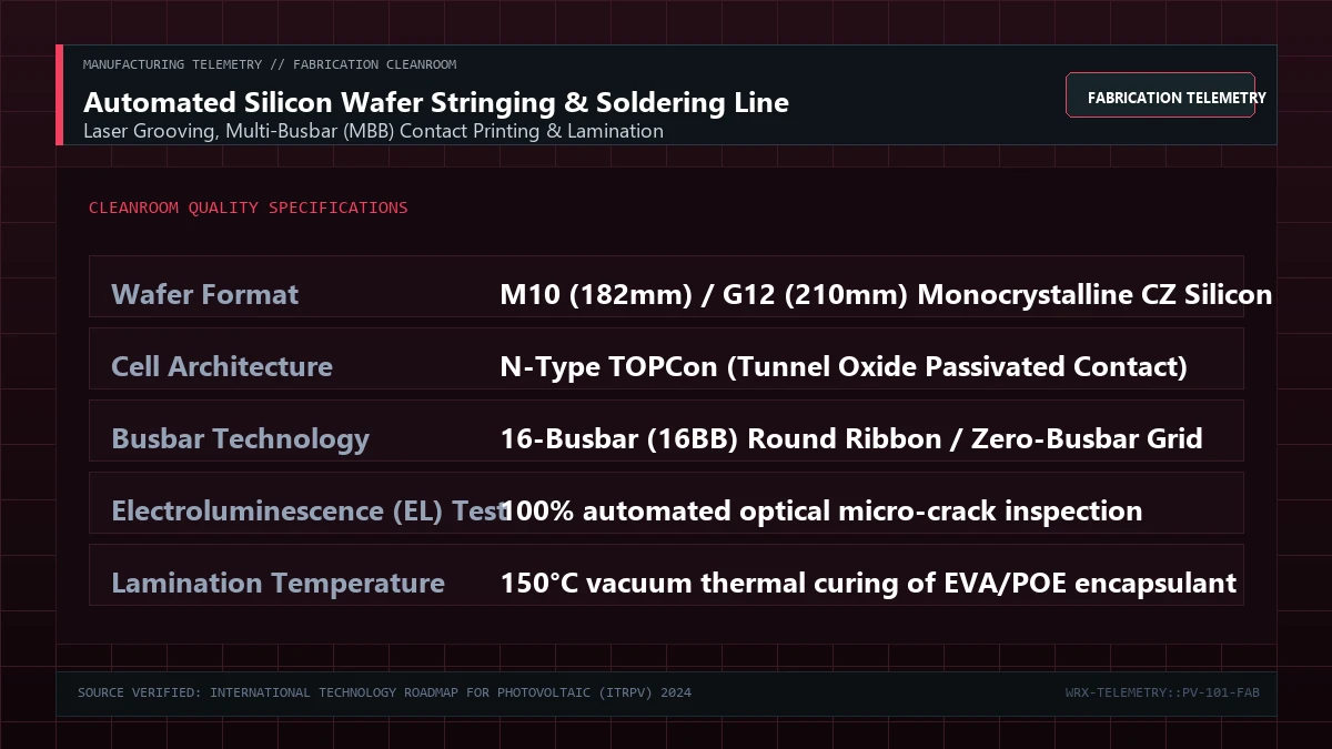
• Front Metallic Grid: Ultra-thin silver contact fingers are screen-printed onto the front sunlit surface of the silicon wafer. These fingers collect free electrons while occupying less than 3% of the surface area to minimize optical shading. Thicker horizontal ribbons called busbars (modern modules use 10 to 16 micro-busbars) collect current from the fingers. • Rear Back Contact: A continuous layer of screen-printed aluminum or silver covers the back of the wafer, collecting the positive holes. • Direct Current (DC) Flow: When an electrical load (such as an inverter or battery) is connected between the front and rear contacts, electrons flow through the external circuit, performing electrical work before returning to the P-side rear contact to recombine with holes, completing the circuit.
Cell-to-Module Integration: A single silicon solar cell produces a voltage of approximately 0.55 to 0.62 Volts regardless of its physical surface area. Because 0.6V is insufficient to run household equipment, manufacturers string multiple cells together in series—typically 60, 72, 108, or 144 half-cut cells. Wiring cells in series adds their voltages together ($0.6\text{V} \times 72 = 43.2\text{V}$), producing a commercially usable operating voltage between 35V and 45V DC.
Step 5: The Inverter: Transforming Direct Current into Alternating Current
The electricity generated by solar modules is Direct Current (DC), where electrons flow steadily in one direction. However, electrical power grids, household lighting, refrigeration compressors, and consumer electronics run on Alternating Current (AC), where electrical current rapidly oscillates back and forth at 50 or 60 cycles per second (Hertz) at 120V or 240V.
The inverter bridges this gap through high-speed power electronics:
1. Maximum Power Point Tracking (MPPT): An intelligent microprocessor continuously sweeps the panel's Current-Voltage (I-V) curve hundreds of times per second. By dynamically tuning electrical resistance, the MPPT ensures the solar array always operates at the precise knee of the curve where Voltage multiplied by Current yields maximum possible wattage ($P_{\text{max}} = V_{\text{mp}} \times I_{\text{mp}}$). 2. Pulse Width Modulation (PWM): Modern inverters use solid-state transistors called Insulated Gate Bipolar Transistors (IGBTs) or Silicon Carbide (SiC) MOSFETs switching on and off thousands of times per second to chop the incoming DC voltage into high-frequency pulses of variable width. 3. Inductive Filtering: The pulsed square-wave output passes through inductors and capacitors that smooth the high-frequency pulses into a clean, distortion-free pure sine wave synchronized with the grid's exact voltage, phase angle, and frequency. 4. Bi-Directional Net Metering: The synchronized AC power flows directly into your home's main breaker panel. If your appliances consume 2,000 Watts while your solar array is generating 5,000 Watts, the home consumes 2,000W locally and exports the surplus 3,000W through your bi-directional utility meter into the neighborhood power grid.
Efficiency Limits: The Shockley-Queisser Limit and Beyond
Why doesn't a solar panel convert 100% of sunlight into electricity? In 1961, physicists William Shockley and Hans Queisser calculated the fundamental theoretical efficiency ceiling for a single-junction solar cell, known as the Shockley-Queisser Limit:
For a single crystalline silicon P-N junction, the maximum theoretical conversion efficiency is approximately 29.4%. The losses stem from fundamental thermodynamic laws: • Spectrum Mismatch Loss (~50%): Sunlight consists of multiple photon wavelengths. Photons with energy below 1.12 eV cannot excite electrons and pass through unconverted (~19% loss). Photons with energy far above 1.12 eV (like blue and UV light) excite electrons, but the excess energy above the bandgap is instantly shed as thermal lattice heat through carrier thermalization (~33% loss). • Radiative Recombination (~10%): Some electrons inevitably recombine with holes before reaching the metallic contacts, emitting photons. • Electrical Resistance and Shading (~5%): Contact resistance and front busbar shadowing.
Overcoming the Limit with Tandem Cells: To break through the single-junction ceiling, researchers have developed Tandem Solar Cells. By stacking a high-bandgap perovskite cell on top of a low-bandgap silicon cell, the top layer absorbs high-energy blue photons efficiently, while the bottom silicon layer captures lower-energy red and infrared photons. In laboratory testing, perovskite-silicon tandem cells have achieved efficiencies exceeding 33.9%, paving the way for next-generation commercial rooftop panels.
Frequently Asked Questions
What is the photovoltaic effect in simple terms?
The photovoltaic effect is the process where a material (usually silicon) absorbs light particles (photons) and knocks electrons free from atoms, creating an electric current when connected to an external circuit.
Why do solar panels need an inverter?
Solar panels generate Direct Current (DC) electricity, where electrons flow in one direction. However, electrical grids and home appliances use Alternating Current (AC), which reverses direction 50 or 60 times per second. The inverter converts DC to AC and synchronizes with the grid.
Do solar panels wear out or run out of electrons?
No. Solar panels never 'run out' of electrons because the system operates in a closed continuous circuit: electrons that leave the panel flow through your home's appliances and return to the back of the solar panel to be excited again by new photons.
What is the average efficiency of a modern solar panel?
Modern residential monocrystalline solar panels (such as N-type TOPCon and Heterojunction modules) achieve commercial conversion efficiencies between 21% and 24%, meaning they convert nearly a quarter of all incident sunlight into usable electricity.